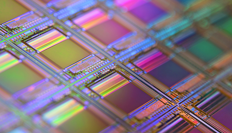
Wafer Bumping
Wafer bumping can provide significant performancekeo bong da, outline dimensions, and overall cost advantages in semiconductor packaging. Extensive experience in numerous alloy mate…

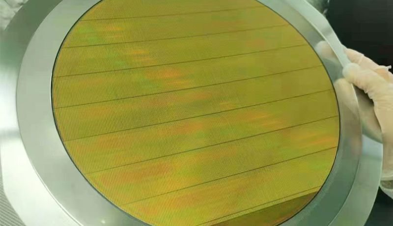
Chip Probing
Chip Probing is to needle test each grain on the waferkeo bong da, and the probe is equipped with gold wire made of gold wire on the detection head, and the contact (pad) on the gra…
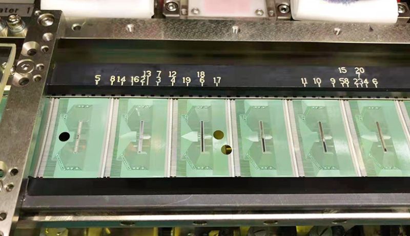
Chip On Glass(COG)
The main purpose of Chip On Glass packaging production line is to divide the wafer into the state of the grainkeo bong da, and the process technology used includes grinding, cutting…
Thin-film over-the-envelope (COF)
COF is a technology that combines Flip Chip Bonding on a Flexible Printed Circuit board (FPC) substrate. That iskeo bong da, the driver IC and its electronic parts can be directly p…
LCM

Reliability Lab (RA Validated)
Huaxin Zhenbang Testing Center provides environmental reliability experiments such as thermal shock testingkeo bong da, pressure cooker testing (PCT), low-temperature testing, high-…